Prototype Board Types from Breadboards to Custom PCBs
On a prototype, the connections are part of the circuit. Spring contacts, hand-soldered wires and etched copper traces each add their own resistance, capacitance and inductance. They also hold up differently to handling, so the same circuit can behave one way on one build and another on the next. A circuit that runs cleanly on a breadboard can still show noise, timing errors or extra heat on its first PCB. The build method decides which of those effects a prototype can reveal. Some stay hidden until the board resembles the product.
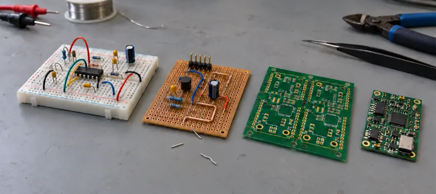
Prototype boards fall into three families based on how their connections are made: solderless breadboards, soldered boards such as perfboard and stripboard, and custom PCB prototypes. Breadboards use reusable spring contacts, soldered boards hold hand-wired joints in place, and custom PCBs carry copper traces fabricated from design files. While component values in a DC or low-frequency circuit are still changing, a breadboard is usually the faster tool. A custom PCB prototype becomes the next step once results depend on layout or fine-pitch packages, or when you need several identical units.
What Is a Prototype Board?
A prototype board is any platform used to build and test an electronic circuit before the design is committed to a production printed circuit board (PCB). It lets engineers confirm that a circuit works, swap parts and take measurements while changes are cheap. A hardware project often moves through more than one type, starting with a quick concept check and ending with a fabricated board close to the production design.
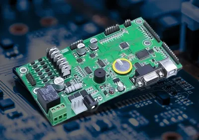
Protoboard, prototyping board and electronic prototype board are other names for the same family. Distributor catalogs file blank perfboard-style products under prototype boards, and many retail listings call them PCB prototype boards. These general-purpose boards are not tied to any one circuit. The term “custom PCB prototype” refers to a board fabricated from your own layout files.
How the Main Prototype Board Types Compare
The table covers five common board types, plus the SMD adapters that connect surface-mount parts to breadboards and hand-wired boards. How a board forms its connections determines how you change it, which component packages it accepts and how closely the finished build matches a production board.
| Board type | Connection method | How changes are made | Component types | Electrical behavior | Typical use |
|---|---|---|---|---|---|
| Solderless breadboard | Spring-clip contacts in five-hole rows | Pull and re-plug leads | Through-hole (THT) parts and jumper wires, surface-mount (SMD) parts on adapters | Suited to DC and low-frequency circuits. Contact and wiring parasitics matter more as signals get faster | Concept checks, early debugging |
| Perfboard | Isolated pads joined by wire or solder bridges | Desolder and rewire | THT, SMD on adapters | Depends on wire length and routing | Permanent one-offs, test fixtures |
| Stripboard | Pre-joined copper strips, cut to separate nodes | Desolder, cut or bridge strips | THT, SMD on adapters | Long parallel strips add copper area and coupling | One-off audio and linear analog builds |
| Solderable breadboard | Breadboard hole pattern in copper | Desolder and rewire | THT, SMD on adapters | Same hole pattern and strip layout as the breadboard, with stable joints | Making a working breadboard layout permanent |
| SMD adapter or breakout board | Package pads routed to 0.1-inch pitch pins | Swap the adapter or rework the part | SMD packages such as SOIC, QFN and QFP | Adds lead length. Thermal pad and decoupling differ from the final layout | Mounting SMD-only parts on a breadboard or perfboard |
| Custom PCB prototype | Fabricated copper traces, usually with plated holes and solder mask | Trace cuts and jumper wires for small fixes, a new revision for layout changes | THT and SMD, including fine-pitch and ball grid array (BGA) | Defined by stack-up and routing, can match the production design | Engineering validation, pilot builds |
The board price is only part of the cost. Hand wiring needs almost no layout preparation, but each unit takes time to wire. Design time for a custom PCB is spent once per revision, and every board in the batch then carries the same copper pattern. Which board type fits depends on what your current build has to prove and how many units your next test needs.
Solderless Breadboards and Their Electrical Limits
A solderless breadboard holds component leads and jumper wires in spring-clip contacts on a 0.1-inch (2.54 mm) grid. Each short row connects five holes, a center channel lets a dual in-line package (DIP) chip straddle both sides, and power rails run along the edges. Ratings vary by model. A common 830-point board, the BusBoard BB830, is rated for 36 V and 2 A (BB830 datasheet). Anything above the board’s voltage rating, including mains-powered stages, belongs on a PCB designed for that voltage.
Stray capacitance between rows amounts to a few picofarads. In a DigiKey TechForum article, an application engineer measured about 2 pF between adjacent five-hole rows, and a second method gave roughly 5 pF. At audio frequencies, the effect was negligible. The author suggests a practical limit of 100 kHz to 1 MHz for signals routed through the contacts. Capacitive reactance falls as frequency rises (XC = 1 / (2πfC)), and even that much capacitance starts to load high-impedance nodes.
The wiring and the board bring their own parasitics. Jumper-wire loops add inductance, contact resistance shifts slightly each time a lead is reinserted, and the board has no continuous ground plane to give return currents a short path. For that reason, Analog Devices’ MT-100 tutorial describes plug-in breadboards and non-clad perforated boards as unsuitable for high-performance or high-frequency analog circuits, where the only effective prototype is often a real PCB layout.
Within those limits, a breadboard handles DC and low-frequency analog circuits well. It suits microcontroller and logic work on short, slow buses such as I2C at 100 or 400 kHz. A working breadboard confirms circuit topology, starting component values and firmware logic. Noise, electromagnetic interference (EMI), thermal behavior and timing margins depend on the product’s PCB layout, which a breadboard cannot reproduce.
Perfboard, Stripboard and Other Soldered Prototype Boards
Soldered prototype boards give up quick changes in exchange for joints that survive handling, transport and field testing. The circuit is still wired by hand, but every connection is a solder joint that stays put.
Perfboard
Perfboard is a sheet of insulating laminate drilled on a 0.1-inch grid. The pad-per-hole version used for soldered builds has a copper pad around each hole and no connections between pads. You join pads point to point with wire, component leads or solder bridges. Plated-through-hole (PTH) versions have pads on both sides, and the plating through each hole anchors them more firmly than pads on a single-sided board.
The laminate matters when parts have to come off again. FR-2 paper-phenolic is the lower-cost option. FR-4 glass-epoxy tolerates repeated soldering heat better, and its pads are less prone to lifting during rework. Perfboard suits permanent one-off builds, test fixtures and small batches of field-test units.
Stripboard
Stripboard joins each row of holes with a continuous copper strip, so part of the wiring is in place before the first component goes in. Veroboard is a well-known trade name for the format. Circuits with a mostly linear signal flow, such as audio stages, simple analog filters and power distribution rails, map well onto the strips and need few extra wires. You separate circuit nodes by cutting the strip at chosen holes.
A cut has to clear the copper completely. Even a thin sliver across the gap keeps the two sides connected. Run a continuity check across every cut before power goes on.
Solderable Breadboard
When a breadboard circuit works and needs to stay together, a solderable breadboard makes it permanent with the least rework. A matching board copies the hole pattern and internal connections of the solderless version, so you can move the parts and wires across hole for hole and solder them in place. Soldered joints do away with contact wear and the resistance shifts that come with reinsertion. The wiring layout does not change, though, and neither does the missing ground plane.
SMD Adapters and Breakout Boards
Many current integrated circuits (ICs) come only in surface-mount packages such as SOIC, QFP and quad flat no-lead (QFN). None of these fits a breadboard or a 0.1-inch grid. An SMD adapter routes the package pads out to 0.1-inch pitch header pins. Some breakout boards also add support parts such as a regulator, decoupling capacitors or pull-up resistors.
On a bare adapter, signal paths get longer and decoupling capacitors end up farther from the supply pins. A QFN’s exposed thermal pad may have little copper beneath it. A regulator can run hotter on the adapter than on the final board, where its pad sits on a copper pour with thermal vias. Temperatures measured on the adapter are a poor guide to the final design.
When to Switch to a Custom PCB Prototype
Move to a custom PCB once your open questions are about the layout, the component packages or unit-to-unit consistency. A breadboard or perfboard is still the faster place to settle circuit topology and starting component values. Changes there take seconds or minutes.
| Trigger | Why a hand-wired build cannot settle it | What a custom PCB prototype adds |
|---|---|---|
| Fast edges, RF or controlled impedance | Wire loops, contact parasitics and the missing reference plane distort fast signals | Trace widths, spacing and stack-up set in the layout, with impedance that can be specified and measured |
| Fine-pitch SMD, QFN or BGA parts | Adapters lengthen leads, BGAs are close to impossible to hand-solder, and hidden joints need X-ray to inspect | Production footprints, stencil printing, reflow and X-ray inspection where needed |
| Mains or other high voltage | Breadboards such as the BB830 are rated for 36 V, and hand wiring leaves conductor spacing undefined | Conductor spacing laid out for the working voltage, following IPC-2221C for general spacing and the product’s safety standard for clearance and creepage |
| Higher current or concentrated heat | The BB830 is rated for 2 A, thin jumper wires add resistance, and there is little copper to pull heat away from hot parts | Copper weight, pour area and thermal vias sized to the load |
| Enclosure, connector and mounting fit | A hand-built board does not share the product’s outline | Final outline, hole positions and connector placement |
| Several identical units | Each hand-wired build differs slightly in wiring | Identical copper on every board for field trials, customer samples and parallel firmware work |
| Electromagnetic compatibility (EMC) pre-compliance | Emissions depend on the product’s own layout and return paths | A representative layout for pre-scans before formal testing |
Radio frequency (RF) boards with tight loss budgets or higher microwave frequencies often move straight to a high-frequency PCB on a low-loss laminate. Controlled-impedance lines on standard FR-4 need a stack-up defined before layout. Fine-pitch BGAs may call for high-density interconnect (HDI) features such as microvias to break out the inner rows of balls.
Does every design need a breadboard stage first? Not when most of the circuit comes from proven reference designs. In that case, you can breadboard only the uncertain part, such as a sensor front end or a low-speed interface, and take the rest of the design into PCB layout.
What a Custom PCB Prototype Can Validate
A custom PCB prototype puts the layout itself under test. Its parasitics, return paths and thermal paths now come from the board you designed.
-
Bare board
For controlled-impedance boards, the fabricator usually measures test coupons from the same panel against the impedance target. Test-fitting the bare board in the enclosure checks the outline and mounting holes.
-
Assembled
You can check connector alignment and whether the footprints and stencil apertures give sound solder joints.
-
Under power
Your team can start on power-integrity and thermal checks: supply noise across the decoupling capacitors, and temperature rise with the copper pours and thermal vias in place.
A small prototype batch says little about production yield.
Bare Boards vs. Assembled Prototypes
Choose bare boards when
- Your team assembles and reworks in-house
- Parts are through-hole or coarse-pitch
- The circuit is expected to change between builds
Choose assembled prototypes when
- The design uses fine-pitch QFNs, BGAs or 01005 passives (0.4 by 0.2 mm)
- You need several identical units at once
- Engineering time is the scarcer resource
Fine-pitch parts need stencil-printed solder paste and reflow, and the assembler can check the hidden joints under BGAs and QFNs by X-ray. Prototype PCB assembly can be full turnkey, partial turnkey or consigned, depending on which parts the assembler sources.
How PCBAIR Builds and Assembles Custom PCB Prototypes
PCBAIR fabricates custom PCB prototypes from one to 20 layers, including HDI, rigid-flex and hybrid RF designs. Trace width and spacing go down to 3 mil (about 0.076 mm), depending on copper weight and stack-up. Every board goes through automated optical inspection (AOI) and 100% bare-board electrical testing. IPC-A-600 Class 2 is the standard acceptance level, with Class 3 available on request. Assembly runs in the same facility and handles 01005 passives and 0.25 mm pitch BGAs.
Including these files and details speeds up the quote:
- Gerber files with NC drill data, or an ODB++ package
- Fabrication notes covering stack-up, impedance targets, laminate, board thickness, copper weight, surface finish and IPC class
- For assembled builds, the bill of materials, pick-and-place (centroid) file and assembly drawing from the same design revision, with do-not-populate parts marked
- Quantity and target turnaround
- Test requirements, such as impedance coupon testing or functional tests
If you are ready to test the layout itself, send the design files. We will reply with a quote and the available lead times.
Prototype Board FAQs
Is a prototype board the same as a breadboard?
A breadboard is one kind of prototype board, but the terms are not always interchangeable. “Prototype board” can mean any platform used to build and test a circuit. Many catalogs use the term for soldered boards such as perfboard. The practical difference is reuse: a solderless breadboard can be rewired on the spot, and a soldered prototype board holds a fixed circuit that survives handling.
Can a breadboard handle high-frequency or RF circuits?
Not reliably. Stray capacitance of about 2 to 5 pF between adjacent rows, jumper-wire inductance and the missing ground plane all distort signals as frequency rises. A DigiKey application engineer who measured that capacitance suggests a practical limit of roughly 100 kHz to 1 MHz. RF and high-speed analog circuits are usually tested on the chip maker’s evaluation board or on a custom PCB with controlled impedance. Another option is dead-bug construction, with parts wired point to point over a solid copper-clad ground plane.
Does a breadboard circuit carry over to a PCB layout?
Only the schematic carries over. The layout starts from scratch on the PCB, with new trace lengths, return paths and decoupling capacitor positions, all planned around the board’s stack-up and parts placement. When you replace a breakout board with the bare chip, the footprint changes and your schematic has to include the support parts the board provided.
How many boards should a first PCB prototype order include?
There is no single right number. A first order usually includes more boards than the working units you need. Spare boards allow for rework on fine-pitch parts and replace any that get damaged during bring-up. They also let hardware and firmware engineers debug in parallel. Per-board fabrication cost falls as quantity rises, and a reorder adds a full fabrication cycle to the schedule.
Does a bare-board electrical test confirm that the circuit works?
No. A bare-board electrical test checks the copper itself, comparing each net against the design data to find opens and shorts. With no components fitted, it cannot show whether the circuit performs its function. Functional verification needs the assembled board, defined operating conditions and pass criteria for each test.
Should a prototype PCB be built to IPC Class 2 or Class 3?
Build it to the same class as the production board whenever its results will be used for qualification or reliability testing. Early functional checks often stay at Class 2. Class 2 covers dedicated-service electronics where continued performance and extended life are required, and it is the usual baseline for industrial and commercial products. Class 3 covers high-performance products where continued operation is critical and downtime cannot be tolerated, such as life-support equipment, and applies tighter acceptance criteria. Those criteria add fabrication and inspection cost. For rigid boards, IPC-6012F sets the class requirements, and IPC-A-600M, the current acceptability standard for bare printed boards, defines the matching inspection criteria.