
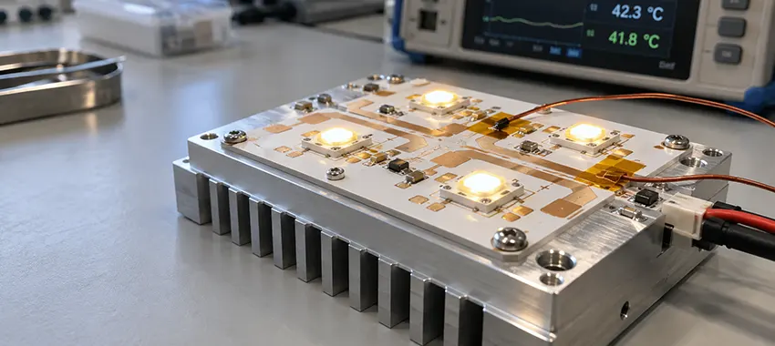
How to Choose the Right Ceramic PCB for LED Applications
Engineers usually turn to ceramic PCBs when an LED design starts running into thermal limits. Common triggers are heat concentrated in a small area, too little board space to spread it, or a dielectric layer in the existing board that takes up too much of the thermal budget. A higher-conductivity substrate reduces only one part of the temperature rise between the surrounding air and the LED junction, so how much it helps depends on the substrate’s share of the total thermal resistance.
Set the LED junction-temperature target, work out how much thermal resistance the heat path can afford, and match the ceramic, its thickness, and the metallization to that limit. Alumina (Al2O3) is often sufficient, at lower cost, when the whole path stays within the thermal budget. The higher cost of aluminum nitride (AlN) is easier to justify when the ceramic layer accounts for a large share of the total thermal resistance. Verify the selection on an assembled prototype.
When Does a Ceramic PCB Make Sense for an LED Design?
A ceramic PCB is worth considering when the insulating layer of a conventional LED board becomes the bottleneck in the heat path, or when the design calls for ceramic’s lower coefficient of thermal expansion (CTE) or its inorganic insulating layer. Heat flux, the heat passing through each square centimeter of the board, is one of the key numbers to watch.
FR-4 and aluminum metal-core PCBs (MCPCBs, often called aluminum PCBs) still suit many LED products.
Ceramic PCB vs. Aluminum PCB for LEDs
If your aluminum MCPCB already holds the LED junction at or below its temperature target under representative operating conditions, the extra cost of ceramic buys margin the design does not need. Once the MCPCB’s dielectric takes a large share of the total thermal resistance and little temperature margin remains, ceramic starts to make a measurable difference. A smaller heat source raises that share, since the resistance of the board layers grows as the area shrinks.
| Design consideration | Aluminum MCPCB | Ceramic PCB |
|---|---|---|
| Electrical insulation | A thin polymer-based dielectric between the copper and the aluminum base | The ceramic substrate itself |
| Heat spreading | Handled by the aluminum base | AlN spreads heat better than alumina. Copper geometry still shapes lateral spreading on both |
| Board-level thermal resistance | Often dominated by the dielectric | Largely set by the ceramic’s thermal conductivity and thickness |
What Matters Most When Selecting a Ceramic PCB for LEDs?
The starting point is the thermal budget: the temperature rise allowed between the highest ambient temperature the product will see and the LED’s junction-temperature target. Dividing that temperature rise by the heat load Q gives the maximum allowable thermal resistance of the complete heat path:
Rth,max = (Tj,target − Ta,max) / Q
A 60 K budget allows about 20 K/W for 3 W of heat and only 2 K/W for 30 W.
How much of that limit the board layers use tells you whether you need ceramic at all and, if so, which one.
In simplified form, the heat path looks like this:
- LED junction
- LED package
- Solder joint
- Copper circuit
- Ceramic
- Thermal interface material
- Heat sink
- Ambient air
The layers and interfaces sit in series, so their thermal resistances add up, and so do the temperature drops across them. As with resistors in series, the largest resistance produces the largest temperature drop.
For a uniform layer under one-dimensional, steady-state conduction, thermal resistance is the layer thickness t divided by the product of thermal conductivity k and heat-transfer area A: Rth = t / (k × A). The table below applies that formula to three insulating layers, first with 10 W flowing through a 1 cm² path and then with the same 10 W concentrated into 0.25 cm².
| Insulating layer | Thickness | k, W/(m·K) | Rth for 1 cm², K/W | Drop at 10 W/cm², K | Drop at 40 W/cm², K |
|---|---|---|---|---|---|
| MCPCB dielectric | 100 µm | 3 | 0.33 | 3.3 | 13 |
| Alumina | 0.63 mm | 24 | 0.26 | 2.6 | 10.5 |
| AlN | 0.63 mm | 170 | 0.04 | 0.4 | 1.5 |
In this example, the alumina layer offers slightly less resistance than the dielectric, even though it is more than six times as thick. Because the estimate leaves out spreading, it overstates the resistance under small heat sources.
The ceramic selection draws on five inputs:
-
LED heat load and heat flux
The heat load is the electrical input power minus the power that leaves as light. For early estimates, Cree LED’s XLamp thermal management guide suggests conservatively assuming that 75% of the input power becomes heat. Efficiency data for the specific LED can refine that figure. Pushing the same load through a smaller area raises heat flux, and the substrate temperature climbs with it.
-
Junction-temperature target
The LED datasheet gives the maximum junction temperature. Many designs aim lower for better lumen maintenance.
-
Ceramic thickness
For a given material and area, through-plane resistance rises with ceramic thickness. A thinner layer lowers it, at the cost of a shorter insulation path, lower board stiffness, and less handling margin.
-
Electrical isolation
The required isolation comes from the LED string voltage, the driver topology, and the safety standard that applies to the end product. It sets the minimum ceramic thickness, conductor spacing, and dielectric strength.
-
Temperature cycling and mounting
Copper, ceramic, solder, and the LED package or die expand by different amounts as temperature changes. The CTE mismatch loads the copper-to-ceramic bond and the solder joints on every cycle, and the board’s supports and fasteners add stress of their own.
The switch-over point from alumina to AlN varies from design to design. LED spacing, board size, package thermal resistance, heat-sink performance, and ambient temperature can each move it, even at the same nominal LED power.
Alumina vs. Aluminum Nitride for LED Ceramic PCBs
For designs where the ceramic layer is only a small part of the total thermal resistance, alumina does the job at lower cost. AlN makes the bigger difference once that share grows, typically because heat is concentrated in a small area.
Alumina (Al2O3) has long been the standard ceramic substrate material in electronics and is the most common base for thick-film circuits.
Aluminum nitride (AlN) has about seven times the thermal conductivity of alumina in the grades compared below and a lower CTE. Whether that lower CTE helps depends on how closely it matches the LED die or package on the board.
| Selection factor | Alumina (Al2O3) | Aluminum nitride (AlN) | What it changes |
|---|---|---|---|
| Thermal conductivity at 20°C | 24 W/(m·K) | 170 W/(m·K) | The ceramic layer’s share of the thermal resistance |
| CTE, 20–300°C | 6.8 ppm/K | 4.7 ppm/K | Dimensional mismatch during temperature cycling |
| Material cost | Lower | Higher | Whether the thermal benefit justifies the added material cost |
Alumina conductivity varies with purity and formulation. A 92% grade offered for thick-film circuits, for example, is listed at 16 W/(m·K), well below the figure in the table. The quotation and the thermal model need to reference the same grade and conductivity value.
The rest of the thermal path and the margin left in the budget decide how much the conductivity gap matters. In the example above, switching from alumina to AlN saves about 2 K at 10 W/cm² but about 9 K at 40 W/cm². With ample margin, a 2 K reduction may not change the material choice, especially when most of the rise sits in the LED package, solder joint, thermal interface material, and heat sink. Close to the junction-temperature target, even 2 K can matter, and 9 K is far more likely to decide it.
How Metallization Affects Ceramic LED PCB Design
The ceramic forms the insulating base, and the metallization process builds the circuit on it. The process determines the copper thickness, the minimum line width and spacing, the current the conductors can carry, and which surface finishes and assembly methods it supports. On an LED board, those limits decide how precisely small pads can be placed and how well heat is drawn away from each emitter.
Direct plated copper (DPC) creates the circuit by electroplating copper inside a photoresist pattern on a thin sputtered seed layer. Because only that seed layer needs etching afterward, the conductor walls follow the drawn pattern closely.
DPC suits LED submounts and compact LED boards that need fine pads, narrow gaps between conductors, or accurate pad placement. Achievable line width and spacing depend on the required copper thickness and the fabricator’s process.
Direct bond copper (DBC), also called direct bonded copper, joins copper foil to alumina or surface-oxidized AlN at high temperature. The copper is generally a few tenths of a millimeter thick. Copper that thick carries high current and spreads heat across the substrate.
Thick copper is normally patterned by wet etching, and the etchant cuts sideways as well as down. Each etched conductor ends up narrower at the top than at the base, so the spacing between conductors has to grow with copper thickness.
Thick-film ceramic circuits are built from conductive pastes that are screen-printed onto the ceramic and then fired. Resistors can be printed alongside the conductors, and printed dielectric layers with filled vias allow multilayer routing on a single substrate. The fired conductors are thinner and less conductive than plated or bonded copper.
| Construction | Typical fit on LED boards | Key design constraint |
|---|---|---|
| DPC | Fine pads, narrow gaps, and accurate pad placement | Thinner copper than DBC |
| DBC | Thick copper for high current and lateral heat spreading | Spacing must widen as copper thickens |
| Thick-film | Printed resistors and multilayer routing on one substrate | Lower current capacity |
Ceramic PCB Requirements by LED Application
LED applications differ in how much heat they produce, how much room the board gets, and what mechanical loads it must tolerate.
| LED application | Main design concern | Ceramic PCB priority | What still needs verification |
|---|---|---|---|
| High-power LED module | Heat concentrated around one or more emitters | Through-plane thermal resistance and lateral heat spreading | Junction temperature with the actual heat sink and drive current |
| COB array | Many dies packed into a small emitting area | Substrate conductivity, die attach, and conductor layout | Temperature spread across the array |
| UV LED | Low conversion efficiency and UV exposure of nearby materials | Thermal path, UV-stable materials, and compatible metallization | The LED maker’s assembly and operating limits |
| Automotive lighting | Temperature cycling, vibration, and mounting stress | CTE mismatch, flat board support, and solder-joint fatigue | AEC-Q102 qualification of the LEDs and the vehicle maker’s test requirements |
COB Arrays
In a COB array, heat from neighboring dies overlaps, so the dies near the center run hotter than those along the edges. Closer die spacing raises junction temperature across the array, with the largest rise at the center.
A higher-conductivity substrate narrows the temperature spread between the hottest and coolest dies, which is one reason to consider AlN for COB designs. A thermal model, or a thermal image of the assembled array, shows the actual distribution.
UV LEDs
UV-C LEDs turn far less of their input into light than white LEDs do. In March 2026, Stanley Electric reported 265 nm sample devices reaching 7.5% wall-plug efficiency. Even at that level, more than 90% of the input ends up as heat, well above the 75% early-estimate figure for visible LEDs.
Near the emitter, UV exposure also ages organic materials. Solder mask, adhesives, and encapsulants in that area should therefore be checked for UV resistance, along with the LED maker’s soldering and metallization requirements. Alumina and AlN are inorganic and are not subject to that kind of UV aging.
Automotive LEDs and Mounting Stress
Vehicle lamps expose LED boards to wide temperature swings. For the LEDs themselves, the relevant AEC qualification standard is AEC-Q102, which requires a minimum temperature range from −40°C to the part’s maximum operating temperature. The board and the finished lamp are tested separately to the vehicle maker’s requirements, and temperature cycling across that range repeatedly loads the copper, ceramic, and solder interfaces because their CTEs differ.
Mounting stress can crack ceramic parts even when the thermal design is sound. Cree LED’s failure analysis of LED luminaires traced dim, flickering, or unlit ceramic-based LEDs to cracks that formed when the board bent during screw tightening, on uneven mounting surfaces, or during depaneling.
On boards held by an even number of screws, the cracks ran perpendicular to the line between the screw holes. That analysis covered ceramic LED packages on conventional boards. Ceramic PCB substrates are brittle too and tolerate very little bending, and the same mounting loads act on them directly.
How Do You Validate a Ceramic LED PCB Before Production?
A practical validation sequence for a new ceramic LED PCB is:
- Thermal estimate or simulation
- Prototype PCB
- Assembled module in the final heat sink and enclosure
- Steady-state measurement
- Reliability testing where required
- Design release
If the prototype runs hotter than expected, the measurement itself is the first thing to check. Light falling on the thermocouple bead, or on adhesive that spills onto the package or blocks its side emission, can push the reading up. The thermocouple bead and its adhesive belong outside the light path.
With a sound measurement, the investigation moves to the heat path: LED spacing, copper layout, solder coverage under the thermal pad, the thermal interface material, heat-sink contact and mounting pressure, and airflow.
Ceramic PCB Manufacturing for LED Applications
PCBAIR provides ceramic PCB manufacturing for LED applications, from prototype builds through production. Before fabrication, PCBAIR’s engineering team reviews your fabrication data, LED package requirements, and operating conditions, then checks the ceramic material, copper thickness, surface finish, and assembly method against those requirements and PCBAIR’s process capability.
To start a review, send us your Gerber files, fabrication drawing, bill of materials (BOM), LED part numbers, operating conditions, prototype quantity, and expected production volume. If a specification is still open, include the operating requirement behind it.
Frequently Asked Questions
Does a ceramic PCB eliminate the need for a heat sink?
Usually not. A ceramic PCB lowers the thermal resistance between the LED and the parts that carry heat away. The heat still has to leave the assembly through a heat sink or another external surface, and a small ceramic board has very little surface area of its own.
Whether you need a heat sink depends on the heat load, board area, ambient temperature, enclosure, and your junction-temperature target.
What surface finish is used on a ceramic PCB for LEDs?
It depends on the metallization and on how the parts are attached. For copper-metallized boards such as DPC and DBC, common options are ENIG (electroless nickel immersion gold), ENEPIG (electroless nickel electroless palladium immersion gold), and electrolytic nickel-gold.
IPC-4552 covers ENIG. IPC-4556 covers ENEPIG and lists it as suitable for soldering and for gold, aluminum, and copper wire bonding. Boards that carry both soldered LEDs and wire-bonded dies can use one finish for both.
Is a ceramic substrate the same as a ceramic PCB?
Not quite. A ceramic substrate is the insulating base material, such as alumina or aluminum nitride. A ceramic PCB adds the conductive circuit, along with any vias and surface finish the assembly needs.
Supplier catalogs and technical papers often use the word substrate for metallized products such as DBC and DPC boards. A quotation should make clear whether substrate means bare ceramic or a finished metallized circuit.