Your Reliable PCB Manufacturing Partner

We have over a decade of experience taking projects from prototype to production, delivering quality-checked, IPC-compliant boards on time for a confident launch.

CONTACT US NOW

PCB Fabrication & Manufacturing Services

Bringing a design to life requires more than a supplier—it requires a partner. We provide complete PCB fabrication and assembly services, from rapid prototypes to mass production. Our facilities are equipped to handle everything from standard single-layer boards to complex HDI and rigid-flex designs, ensuring we can meet your project’s demands.

Our expertise is backed by quality you can trust. Certified to IPC, J-STD, and ISO standards, we build reliable boards for demanding applications like medical and industrial. Our in-house process, which covers everything from fabrication and component sourcing to assembly and testing, simplifies your supply chain and accelerates your time to market. You’ll work directly with our engineers, ensuring clear communication and a team that’s dedicated to getting it right the first time.

PCB Board ICON

Prototype PCBs

Test designs fast. Our rapid prototyping & DFM feedback help you eliminate costly flaws, ensuring a smooth path to production.

Read More
PCB Board ICON

Multilayer PCBs

We fabricate multilayer PCBs up to 40 layers with options for blind/buried vias, impedance control and high‑Tg materials.

Read More
PCB Board ICON

Flexible PCBs

We manufacture single to multilayer flex circuits with stiffener and coverlay options, and offer impedance control for high-speed designs.

Read More
PCB Board ICON

Rigid‑flex PCBs

We engineer custom rigid-flex boards, using 3D modeling to ensure reliable stack-ups for dynamic bending in compact, high-shock environments.

Read More
PCB Board ICON

Metal core PCBs

We manufacture MCPCBs for thermal control in high-power LEDs, power converters & automotive lighting, offering single & multilayer designs.

Read More
PCB Board ICON

HDI PCBs

We build advanced HDI PCBs, from 1+N+1 to any-layer architectures, using stacked microvias to maximize your design's routing density.

Read More
PCB Board ICON

Heavy Copper PCBs

We build heavy-copper PCBs up to 20 oz for high-current applications, combining different weights to optimize your stack-up.

Read More
PCB Board ICON

High‑frequency PCBs

We build RF boards using Rogers & PTFE, ensuring consistent dielectric properties with controlled impedance and strict process control.

Read More
PCB Board ICON

Ceramic PCBs

We build high-performance ceramic PCBs using thick-film & direct-bonded copper for power electronics, RF modules, and aerospace.

Read More
PCB Board ICON

High‑Tg PCBs

We offer high-Tg boards (170–260 °C) to ensure your board’s reliability during lead-free assembly and high-temperature operation.

Read More
PCB Board ICON

Halogen‑free PCBs

We build with halogen-free laminates, ensuring your design meets RoHS compliance and offers high thermal stability & performance.

Read More
PCB Board ICON

Quick‑turn PCBs

Our express service delivers rigid PCB prototypes in as fast as 24 hours, with flex and rigid-flex boards in around 7 days.

Read More

Our PCB Manufacturing Capabilities

We’ve organized our manufacturing specs into clear tabs, so you can quickly review our capabilities for each board category.

Category Attribute Standard Capability
(Cost-Effective & Fast)
Advanced Capability
(Contact for Quote)
General Specs Layer Count 2 – 10 Layers 12 – 40 Layers
Material FR-4 (Tg 130-140°C), FR-4 (Tg 150-160°C) FR-4 (High-Tg 170-180°C), Rogers, Isola, Panasonic, Shengyi
Board Thickness 1.0mm, 1.2mm, 1.6mm (±10%) 0.2mm – 6.0mm (±10%)
Max. Board Dimensions 500 x 500 mm 600 x 1100 mm
Conductor Specs Finished Copper Weight 1 oz (35μm), 2 oz (70μm) 0.5 oz (18μm), Heavy Copper (3-20 oz)
Min. Trace / Space 4 / 4 mil (0.1 / 0.1 mm) 2.5 / 2.5 mil (0.065 / 0.065 mm)
Drilling Specs Min. Mechanical Drill 0.25mm (10 mil) 0.15mm (6 mil)
Min. Laser Drill N/A 0.075mm (3 mil) (For HDI)
Aspect Ratio 8:1 16:1
Via Type Through-hole Vias Blind Vias, Buried Vias, Via-in-Pad, Microvias
Solder Mask Solder Mask Type Liquid Photoimageable (LPI) LPI
Solder Mask Colors Green, White, Black Blue, Red, Yellow, Matte Green, Matte Black
Min. Solder Mask Dam 4 mil (0.1mm) 3 mil (0.075mm)
Silkscreen Silkscreen Colors White Black, Yellow, Red, Blue
Min. Character Height 30 mil (0.762mm) 25 mil (0.635mm)
Surface Finish Standard Finishes HASL (Leaded), HASL (Lead-Free) ENIG (Immersion Gold), Immersion Silver, Immersion Tin, OSP
Advanced Finishes N/A ENEPIG (Immersion Gold Palladium), Hard Gold, Carbon Ink
Special Processes Impedance Control ±10% ±5%
HDI (High Density) N/A 1+N+1, 2+N+2, Any Layer Interconnect (ALIC)
Other Processes N/A Edge Plating, Castellated Holes, Countersinks/Counterbores, Gold Fingers
Category Attribute Standard Capability
(Cost-Effective & Fast)
Advanced Capability
(Contact for Quote)
General Specs Layer Count 1 – 4 Layers 6 – 8 Layers
Construction Type Adhesive Based Adhesiveless
Base Material Polyimide (PI) – 1 mil, 2 mil Polyimide (PI) – 0.5 mil, High-Performance PI
Conductor Specs Base Copper Weight 0.5 oz (18μm), 1 oz (35μm) 1/3 oz (12μm), 2 oz (70μm)
Min. Trace / Space 4 / 4 mil (0.1 / 0.1 mm) 2 / 2 mil (0.05 / 0.05 mm)
Cover & Finish Coverlay / Solder Mask Polyimide Coverlay (1 mil), Flexible LPI Solder Mask Polyimide Coverlay (0.5 mil), Matte Black/White LPI
Surface Finishes ENIG (Immersion Gold) ENEPIG, Hard Gold (for fingers), OSP
Silkscreen White, Black Yellow, Blue
Reinforcement & Mechanical Stiffener Type Polyimide (PI), FR-4 Stainless Steel, Aluminum
Stiffener Thickness 0.1mm – 1.0mm Up to 2.0mm
Outline Method Die Punching, Laser Cutting Plasma Cutting, Contour Routing
Special Processes Impedance Control ±10% ±5%
EMI Shielding N/A Silver Ink Shielding, Cross-Hatched Copper Shield
Min. Bend Radius 10x Circuit Thickness (Dynamic) 6x Circuit Thickness (Static)
Category Attribute Standard Capability
(Cost-Effective & Fast)
Advanced Capability
(Contact for Quote)
General Specs Total Layer Count 4 – 12 Layers 14 – 20+ Layers
Flex Layer Count 1 – 2 Flex Layers 4 – 8 Flex Layers
Rigid Material FR-4 (Tg 150-160°C) High-Tg FR-4 (Tg 170-180°C), Halogen-Free
Flex Material Adhesive Based Polyimide (PI) Adhesiveless Polyimide (PI)
Conductor & Lamination Base Copper Weight 0.5 oz (18μm), 1 oz (35μm) 1/3 oz (12μm), 2 oz (70μm)
Min. Trace / Space 4 / 4 mil (0.1 / 0.1 mm) 3 / 3 mil (0.075 / 0.075 mm)
Lamination Type Bondply / Prepreg Lamination Adhesiveless Bonding, Air Gap Construction
Mechanical & Finish Min. Mechanical Drill 0.2mm (8 mil) 0.15mm (6 mil)
Via Type Through-hole (Rigid Sections) Blind/Buried Vias, Vias Spanning Rigid-Flex
Surface Finishes ENIG (Immersion Gold) ENEPIG, Immersion Silver, Hard Gold (for fingers)
Stiffener Support FR-4, PI Stiffeners Stainless Steel, Aluminum Stiffeners
Special Processes Impedance Control ±10% ±5%
Construction Method Standard Lamination “Bookbinder” Construction for high flex cycles
Shielding on Flex N/A Silver Ink Shielding, Cross-Hatched Copper Shield
Category Attribute Standard Capability
(Cost-Effective & Fast)
Advanced Capability
(Contact for Quote)
General Specs Layer Count 1 Layer (Single-Sided) 2 Layers (Double-Sided)
Base Material Aluminum Alloy (5052, 1060) Copper Core, Other Alloys
Overall Board Thickness 1.0mm, 1.2mm, 1.6mm 0.8mm – 3.0mm
Thermal & Electrical Thermal Conductivity 1.0 – 2.0 W/m·K 3.0 – 8.0+ W/m·K
Dielectric Breakdown Voltage 2000V – 4000V AC >6000V AC
Finished Copper Weight 1 oz (35μm), 2 oz (70μm) 3 oz – 10 oz (Heavy Copper)
Mechanical Specs Max. Board Dimensions 500 x 600 mm 600 x 1200 mm
Min. Hole Size (Drill) 0.8mm 0.5mm
Outline Profile Method Routing, V-Scoring, Punching N/A
Mechanical Processes N/A Countersinks, Counterbores, Beveling
Solder Mask & Finish Solder Mask Color White (High Reflectivity), Black Green, Custom Colors
Surface Finish HASL (Lead-Free), OSP ENIG (Immersion Gold)
Silkscreen Color Black, White Custom Colors

* N/A indicates this process is available under our Advanced Capability. Please review our Advanced specifications or contact us directly to discuss your requirements.

Certified Quality & Compliance

We build quality into every board we manufacture. This isn’t just a promise; it’s a process, verified by the world’s most recognized standards. For you, this means documented consistency, proven safety, and streamlined regulatory compliance.

ISO 9001 2015 ICON

Our ISO 9001 certification demonstrates our commitment to process control, ensuring consistent, repeatable precision.

IPC-A-610 ICON

We inspect all assemblies to IPC-A-610, the global standard, ensuring they meet Class 1, 2, or 3 visual and performance criteria.

J-STD-001 ICON

By adhering to J-STD-001, we ensure all soldering materials and methods meet strict requirements for strong, defect-free joints.

ISO-13485 ICON

As an ISO 13485 certified manufacturer, we ensure rigorous risk management and full traceability for medical devices.

IATF 16949 2016 ICON

Our IATF 16949 certification drives our zero-defect focus, ensuring robust reliability for your automotive components.

ISO 14001 2015 ICON

We adhere to ISO 14001 to manage our environmental footprint, ensure legal compliance, and improve resource efficiency.

UL Recognition ICON

Our UL recognition for materials (UL 94) and boards (UL 796) meets key safety and flammability standards for your product.

ROHS-ICON

We comply with the RoHS Directive, restricting hazardous materials to ensure your product is safe and globally compliant.

Production Tiers & Lead Time

Service Tier Typical Lead Time Primary Application Cost Advantage Key Value
Prototype & Expedited 24 Hours - 5 Days R&D, functional testing, quick-turn validation Time-to-market driven Speed to Market
Rapidly turn your design into reality
Small-Mid Volume 5 - 10 Working Days Pilot runs, NPI (New Product Introduction), early-market launch Optimal balance of cost & speed The Balanced Choice
Quality, cost, and speed in perfect harmony
Mass Production 12+ Working Days (Scheduled) Mature products, high-volume consumer electronics, industrial control Lowest unit cost via economies of scale Economies of Scale
Reliable, consistent, and cost-competitive production at scale

Detailed Lead Time (For Prototypes & Small Volumes)

Board Complexity Expedited Standard
2-4 Layer Rigid PCB 2-3 Working Days 5-7 Working Days
6-8 Layer Rigid PCB 4-5 Working Days 8-10 Working Days
10-16 Layer / Standard HDI 5-7 Working Days 10-12 Working Days
18+ Layer / Advanced HDI / High-Frequency Materials Contact Us for Custom Quote Contact Us for Custom Quote
Flex / Rigid-Flex PCB 5-7 Working Days 10-12 Working Days
Aluminum PCB 3-4 Working Days 6-8 Working Days
*Note: Lead times are estimated in working days and are subject to final engineering review of your Gerber files. Shipping time is not included.

Why Choose Us?

Getting high-quality boards to your production line shouldn’t be a logistical headache. We operate as your trusted global PCB manufacturer by combining expert DFM engineering that ensures manufacturability with a supply chain that actually works. We simply handle the complexities of fabrication and global shipping so you receive reliable, spec-perfect PCBs exactly when you need them to bring your product to market.

PCB Physical Chemistry Experiment

Total In-House Control

We own the entire production line, with every stage of fabrication completed in our Shenzhen facility. This means you speak directly to the engineers actually building your board, avoiding the delays common with middlemen.

Engineering Support

You don’t just talk to reps; you work with DFM engineers. We perform a detailed, free design review on every file to catch errors before fabrication starts. It’s how we ensure your board is built right the first time.

Customer‑Centred Approach

We prioritize transparency. You receive a firm quote based on your specific technical requirements—such as layer count, finish, and thickness—with zero hidden fees. Plus, a dedicated account manager guides you from initial quote to final delivery.

Our PCB Manufacturing Equipment

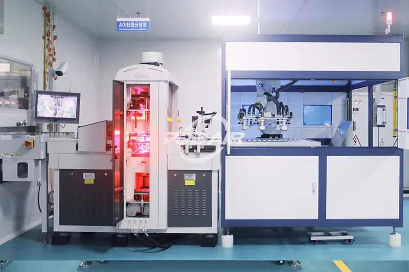
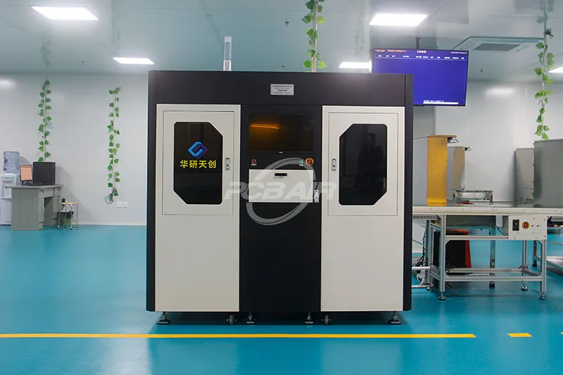
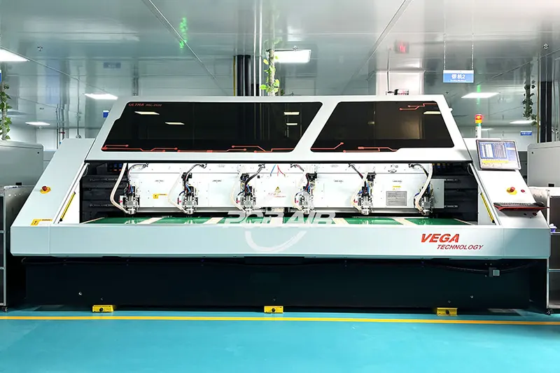
A reliable product requires a flawless foundation. We utilize Laser Direct Imaging (LDI) for high-precision circuit definition, ensuring even the tightest trace widths are etched strictly to spec. We pair this with automated CNC drilling and routing systems that guarantee perfect layer registration and dimensional accuracy.

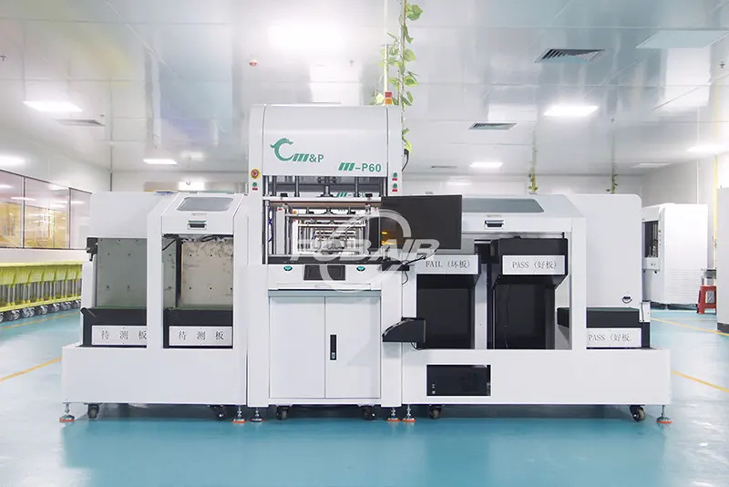
Deep inside the board, consistency is critical. Our computer-controlled plating lines monitor copper deposition in real-time, eliminating the risk of uneven plating in vias or on surfaces. Before shipping, every bare board undergoes 100% E-test and visual inspection, so you never receive a defective substrate.

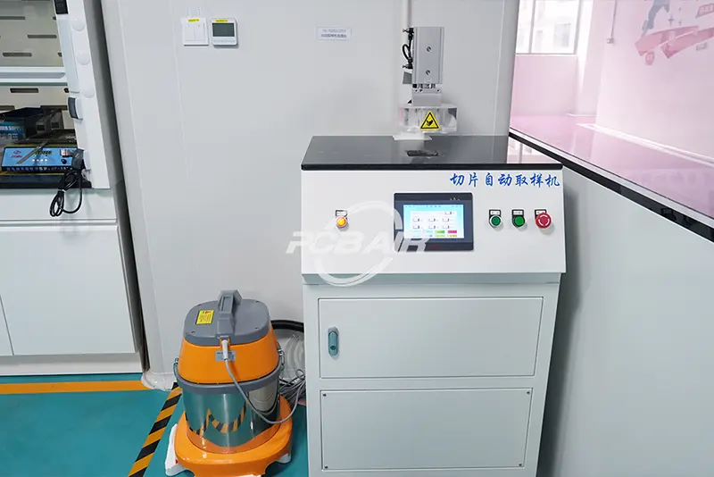
Slicing Automatic Sampling Machine
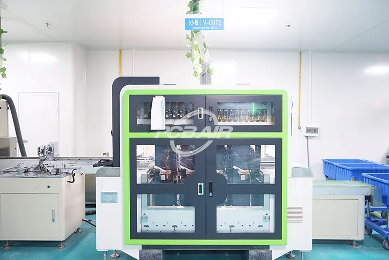
Small Board V-cut Machine
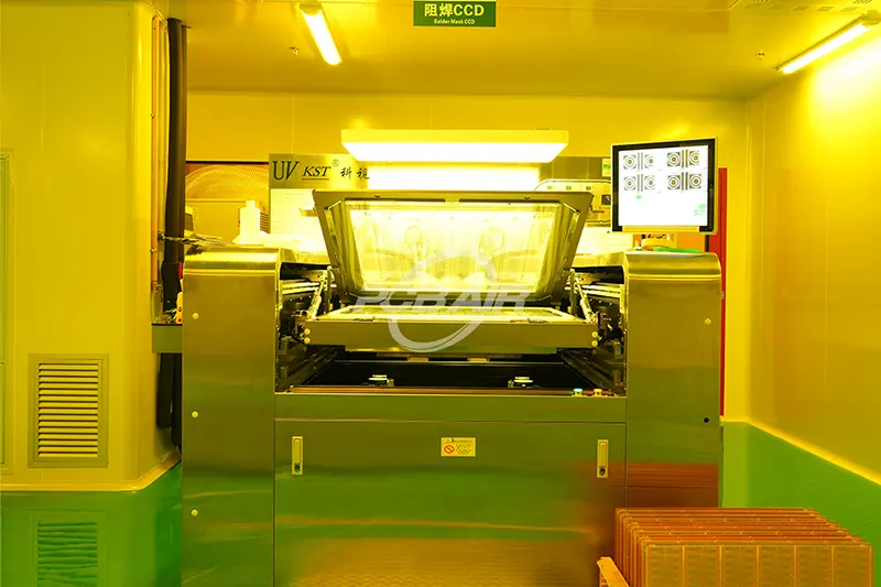
Solder Mask CCD
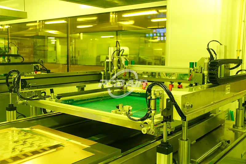
Solder Mask Machine
AOI Analyzing
Automatic Appearance Inspection
Automatic Testing Machine
CNC

Are you looking for a reliable PCB manufacturer for your next project?