Low Loss
With an ultra-low loss factor (Df ~0.001), Rogers laminates preserve signal power more effectively than standard FR-4. This superior characteristic ensures sensitive RF and microwave signals travel with minimal distortion or attenuation.
For high-frequency designs where standard laminates fall short, we build PCBs using Rogers materials. We deliver boards with precise impedance control and minimal signal loss, ensuring superior reliability for your critical RF, 5G, and aerospace applications.
With an ultra-low loss factor (Df ~0.001), Rogers laminates preserve signal power more effectively than standard FR-4. This superior characteristic ensures sensitive RF and microwave signals travel with minimal distortion or attenuation.
The DK of this material remains exceptionally stable across wide frequency and temperature ranges. Unlike FR-4, this prevents impedance shifts, resulting in predictable circuit performance that matches design simulations.
High thermal conductivity lets these materials efficiently dissipate heat from powerful components. This prevents damaging hot spots, ensuring stable, reliable operation for a board that is under significant thermal stress.
Rogers laminates excel in harsh environments. Their low moisture absorption resists humidity, and low outgassing is ideal for vacuum use. A copper-matched thermal expansion rate ensures long-term structural integrity.
Rogers PCBs are built with high-frequency laminates from Rogers Corporation, engineered for applications where standard FR-4 falls short. These advanced substrates, including popular series like RO4350B, deliver exceptionally low signal loss and stable performance at microwave and millimeter-wave frequencies. While more costly than FR-4, their performance makes them essential for demanding fields like 5G infrastructure, satellite communications, and automotive radar. It’s the specialized dielectric material beneath the copper that provides these superior electrical properties.
However, not every layer of your design may require this level of performance. To effectively balance cost and function, a hybrid construction is an excellent solution. This involves using Rogers laminates for RF-critical layers and standard FR-4 for others, such as internal power or ground planes. For example, placing Rogers material on the outer layers ensures low signal loss for your sensitive components, while an FR-4 core keeps the overall board affordable and robust.
We specialize in fabricating these complex hybrid boards, expertly bonding the dissimilar materials without compromising reliability. We source the full range of Rogers materials, helping you select the perfect substrate for your project’s unique demands. All fabrication is completed in-house, and we guarantee quality by performing 100% electrical testing and AOI on every single board before it is delivered to you.
Manufacturing reliable Rogers PCBs is a specialized craft. Because these high-performance materials behave differently than standard FR-4, the process requires special attention to detail. At our facility, we’ve tailored our entire fabrication workflow to handle the unique properties of Rogers materials, ensuring your final board delivers stable, high-frequency performance.
The process begins with selecting the right substrate for your design’s frequency and power requirements. We choose Rogers laminates based on the needed dielectric constant and thickness, including compatible prepregs or adhesives for multilayer designs.
Surface preparation is critical. Rogers materials, especially PTFE-based types like the RT/duroid® series, have very smooth, non-stick surfaces that resist bonding. To solve this, we use advanced surface treatments. A key step is plasma etching, which microscopically roughens and activates the PTFE surface. This ensures that the copper plating and solder mask have a strong, reliable grip, preventing delamination down the line.
Building a multilayer Rogers board, or a Rogers/FR-4 hybrid, involves a carefully controlled lamination cycle. These materials can expand and flex differently than FR-4, so we use optimized temperatures and pressures to press the layers together without causing warping or stress. When creating a hybrid stack-up, we use compatible bonding materials and design the layer arrangement symmetrically to balance out physical forces, resulting in a flat and stable board.
Once laminated, creating the circuitry demands extreme precision. Rogers PCBs often feature controlled-impedance traces where even tiny variations in width can impact performance. We use modern Laser Direct Imaging (LDI) and tightly controlled etching processes to ensure these critical dimensions are met, often holding tolerances within a fraction of a mil.
Drilling these materials also requires a special approach. Since PTFE-based boards are soft, standard drilling can cause tearing or smearing. We use specific drill bits and adjusted parameters (slower speeds and feed rates) to create clean, accurate holes. After drilling, a thorough plasma cleaning removes any residue and prepares the hole walls for a perfect copper plating connection.
Plating the through-holes is a multi-step process. A thin layer of electroless copper is deposited first, followed by electrolytic plating to build up the required thickness for robust via connections.
For the final surface finish, we often recommend ENIG (Electroless Nickel Immersion Gold). It provides a perfectly flat, corrosion-resistant surface that is ideal for soldering sensitive RF components and doesn’t interfere with high-frequency signals.
Rigorous quality control is embedded at every stage to guarantee performance. Our commitment to quality means your board is inspected and tested throughout the manufacturing process, not just at the end. Key checks include:
As an experienced manufacturer of high-frequency PCBs, PCBAIR brings deep expertise to every Rogers project. We handle complex multilayer, hybrid, and rigid-flex designs, keeping all critical processes in-house for total control over quality and lead times. We stock a wide range of Rogers materials to meet your exact specifications, and our engineering team is ready to assist with stack-up design and impedance modeling, making us a reliable partner for even the most demanding RF applications.
With over 10 years in the PCB industry, PCBAIR has established a reliable supply chain that ensures access to premium components at competitive prices. For complex projects needing special materials or advanced technical specifications, our strong manufacturing capabilities enable us to provide cost-effective solutions while maintaining high quality.
We ensure rapid production times, with samples shipped within 24-48 hours and mass production orders delivered within 72-120 hours. Our partnerships with global logistics providers like UPS, EMS, FedEx, DHL, and TNT guarantee prompt and reliable shipping, supported by our digitalized factory management and 90% automation for enhanced efficiency.
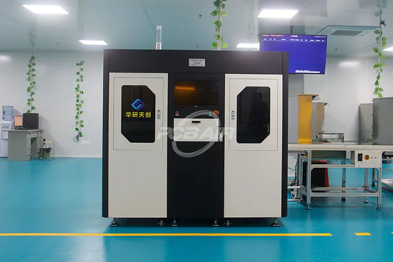
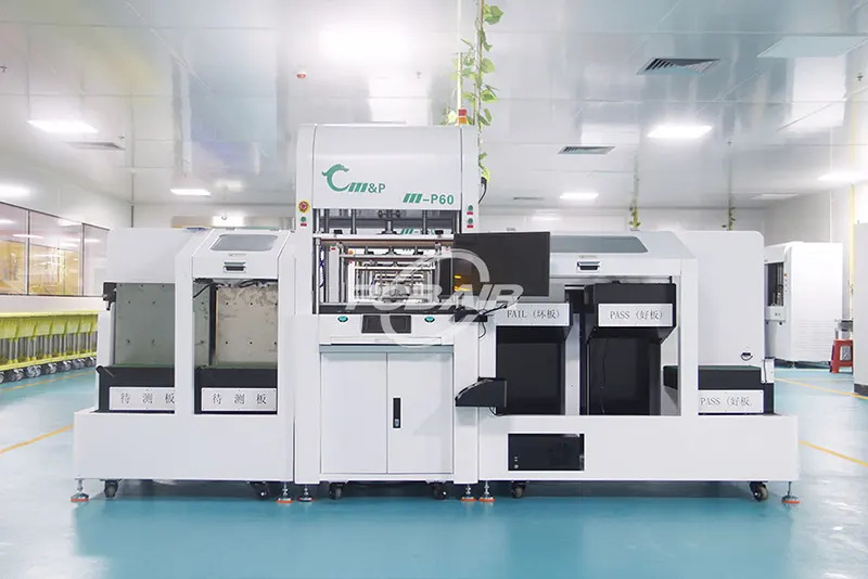
Our rigorous quality inspection begins with incoming material checks. We use AOI to detect defects and X-ray to identify internal issues. Electrical performance testing is performed with advanced automatic test machines and flying probe testers. Before shipment, our dedicated QC team conducts a thorough manual visual inspection to ensure all products meet strict quality standards.
Our experienced sales, order management, and engineering teams provide expert support throughout your project. The sales team handles support and project follow-ups, while the order management team ensures timely quotations and monitors production status. Our engineering team reviews your design files, offering professional advice to optimize production efficiency.
To ensure your PCBs are reliable and perform well, we use high-quality laminate materials. We have built strong partnerships with top suppliers in the industry, including trusted brands like Rogers, Panasonic, Dupont, Arlon, Taconic, Nelco, Isola, Teflon, and more. This means you receive the best materials tailored to your project needs, providing the performance and durability you expect.

By reviewing the following rogers PCB capabilities table, you can briefly understand what we can do.
| Specification | Capability |
|---|---|
| Material Type | Rogers RO4000, RO3000, RT/duroid, TMM series, and other RF laminates. |
| PCB Construction | Multilayer RF, Hybrid/Mixed Dielectric (Rogers + FR-4), Sequential Lamination |
| Dielectric Constant (Dk) Control | Process-controlled to maintain Dk stability within ±0.02 of material specs. |
| Layer Count | 2 – 30 Layers |
| Board Thickness | 0.2mm – 6.0mm (with high-precision thickness control) |
| Base Copper Thickness | ½ OZ to 2 OZ (thicker options available upon engineering review) |
| Minimum Trace / Space | 2/2 Mil |
| Impedance Control | ±7% standard, down to ±5% for critical RF lines |
| Finished Surface | ENIG, ENEPIG (recommended for RF), Immersion Silver, Plating Gold |
| Special Process for PTFE | Plasma Treatment / Sodium Etching (ensures via wall adhesion and reliability) |
| Advanced Via Technology | Back-drilling (stub removal), Blind/Buried Vias, Conductive/Non-conductive Fill |
| Edge Plating / Castellations | Available for RF shielding, grounding, and board-to-board connections |
Please send us a message, and our rogers PCB manufacturing capabilities can help you complete your next project.
Our quality system is certified to ISO 9001 and meets key standards for the medical and automotive sectors. This disciplined approach is applied to every Rogers PCB, beginning with a rigorous inspection of all incoming raw materials to verify their integrity. Throughout production, our in-process controls meticulously monitor every critical stage, from lamination to drilling, ensuring that all design specifications are precisely met and full traceability is maintained for each board.


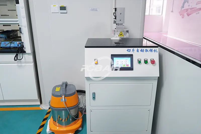
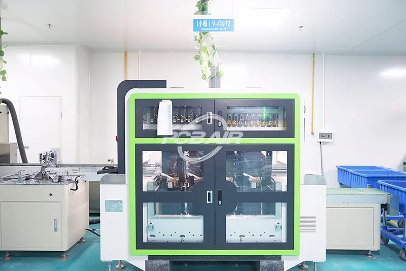
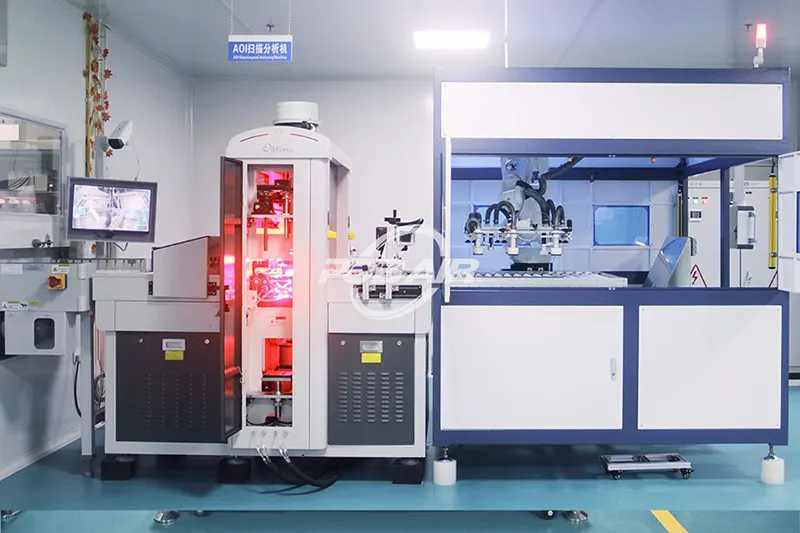
Our 65,000 sqft production campus is equipped with advanced fabrication machinery. We use high-speed CNC machines for both drilling and routing, employing optimized parameters to create clean vias and precise board profiles essential for RF circuits. For multilayer and hybrid constructions, our modern lamination presses apply carefully controlled temperature and pressure profiles, ensuring a solid, void-free bond between all layers.
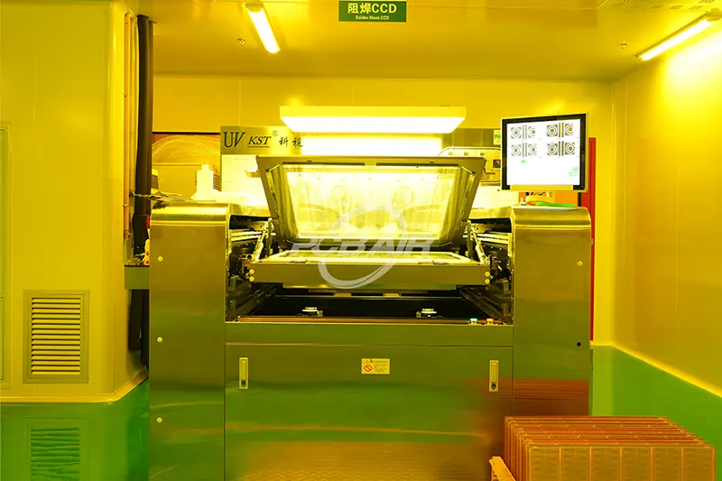
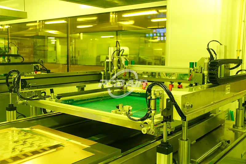
To overcome the challenges of PTFE adhesion, we utilize specialized plasma treatment systems that activate the material’s surface, promoting a strong bond for copper and soldermask. Our automated electroplating lines then deposit a uniform layer of copper, which is critical for consistent signal integrity. These controlled processes are verified by a comprehensive suite of inspection equipment at key stages to ensure each board conforms to its design intent.