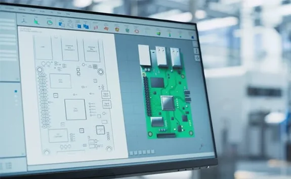
PCB Design & Layout Process at PCBAIR
Our PCB design and layout process transforms your electronic product concepts into production-ready circuit boards. We follow a comprehensive process, ensuring quality and efficiency at every step:
Schematic Capture
We create detailed schematic diagrams from your design ideas using electronic design automation (EDA) tools. These diagrams serve as a precise blueprint for all electrical connections, components, and the BOM.
PCB Component Footprint Creation
Accurate footprints are essential for precise component placement and manufacturability. Our designers select the optimal mounting technology (SMT or THT) and determine the required number of layers (from single to 30-layer designs) based on your project’s specifications. Component placement also takes Design for Manufacturing (DFM) principles into consideration.
PCB Routing
After component placement, we route the physical connections between them. Using the schematic’s netlist and specialized PCB software, our designers ensure efficient signal flow, minimize interference, and maximize performance. We use simulations to proactively identify and resolve potential routing issues, even in complex layouts.
PCB Verification and Analysis
We rigorously verify the PCB design to ensure it meets all specifications, adheres to IPC standards, and achieves EMC compliance, making it ready for manufacturing. This includes:
- Design Rule Checks (DRC): Ensuring the layout adheres to manufacturing constraints.
- Layout Versus Schematic (LVS): Confirming the physical layout matches the schematic connections.
- Signal Integrity Analysis: Evaluating the design for potential signal problems.
For designs incorporating ASICs or FPGAs, we also adhere to relevant design and testing guidelines.
Output – Manufacturing Files
The final step is generating the complete set of manufacturing files, including Gerber files and drill files, ready for PCB fabrication.


